Until recently, floating gate (FG) NAND flash memory technology has been successful in meeting the demand for non-volatile memory (NVM) devices for tablets and smartphoness. However, there is increasing concern in the consumer electronics industry that floating gate NVM might not be able to continue providing higher storage capacities at the ever-lower cost-per-bit requirements that drive the NVM market. The potential for the floating gate approach to “hit the wall” makes research into alternative technologies increasingly critical. Moreover, with more research into newer technologies such as ReRAM (RRAM), new methods of testing are required. These new technologies demand fast I-V pulsing with pulse widths of <10 ns. This document provides solutions on how this testing can be achieved.
NVM Types and Testing
These new NVM types include:
- FG Flash or 3D Flash
- PCM/PCRAM: Phase change memory
- Resistive: ReRam/RRAM, CBRAM
- MRAM: Magnetoresistive RAM
- FeRAM: Ferro-electric RAM
- Spin-transfer torque: STT-RAM or STT-MRAM
- CNT RAM: Carbon-nanotube RAM
These emerging technologies are driving the need for dynamic, simultaneous ultra-fast current and voltage measurements. The Keithley Pulse Measure Unit 4225-PMU/4225-RPM combination provides simultaneous voltage and current measurement, which is important when the dynamic resistance of the material represents the electrical manifestation of the physical mechanism of the bit storage.
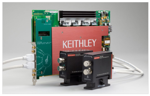
The 4225-PMU Ultra-Fast I-V Module (Figure 1) is a singleslot instrument card for the 4200A-SCS Parameter Analyzer. It has two channels of voltage pulse sourcing with integrated, simultaneous real-time current and voltage measurement for each channel.
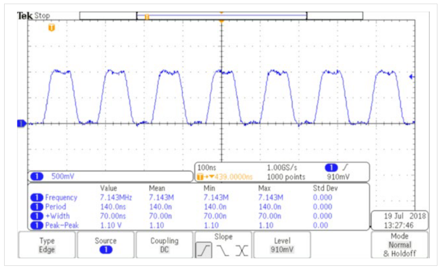
The minimum recommended pulse width with the PMU and the RPMs on the 10 V and 200 mA ranges is 70 ns. Notice the flat top of the waveform in Figure 2, which shows measurement stability.
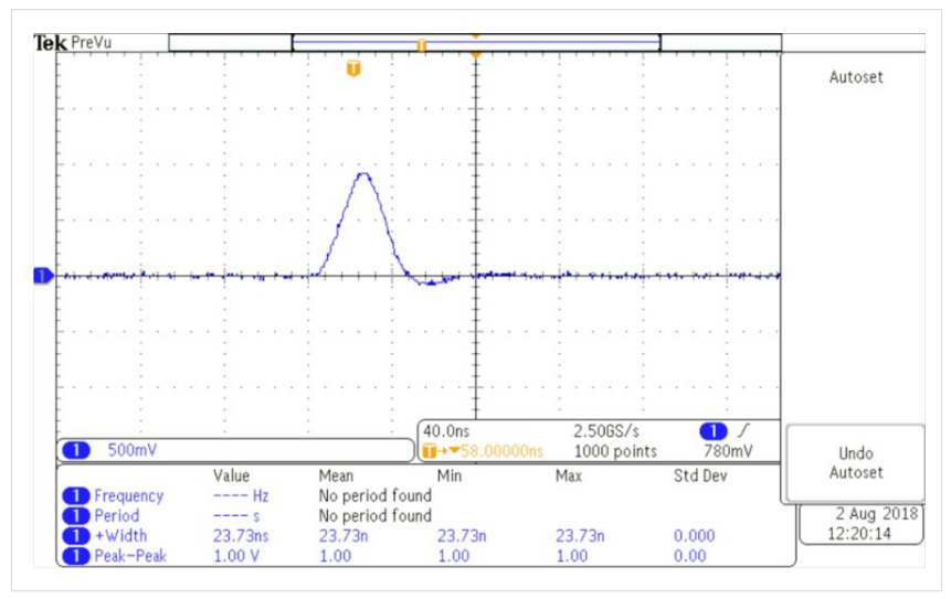
However, the minimum pulse width that could be done for source and measure is 20 ns, as shown in Figure 3.
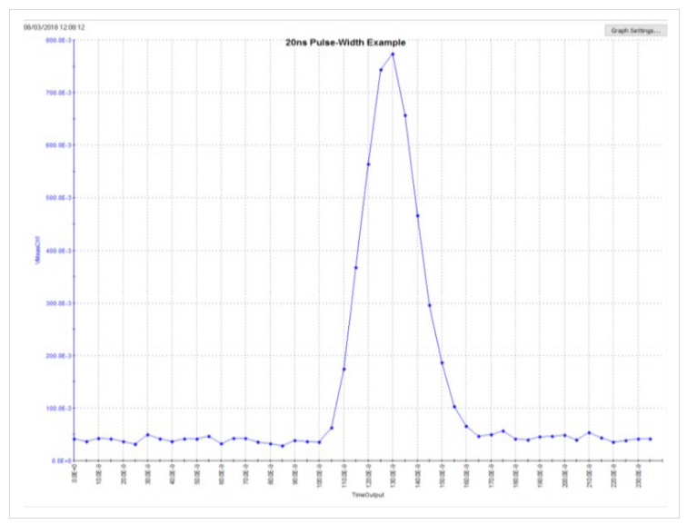
Moreover, the PMU has the capability of measuring at 200 mega-samples/second or every 5 ns, which is shown in Figure 4.
Alternative NVM Testing
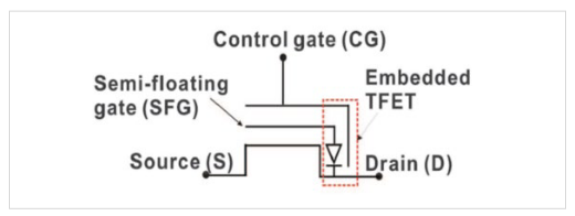
New types of transistor technology are emerging and being used with flash memory. Figure 5 shows a semi-floating gate (SFG) transistor. A p-n junction diode between the floating gate (FG) and drain makes the FG semi-floating. The transistor uses an embedded tunneling field-effect transistor for charging and discharging the semi-floating gate. This transistor operates at low voltages (≤2.0 V), with a large threshold voltage window of 3.1 V, and can achieve ultra–high-speed writing operations (on time scales of ~1 ns). Therefore, fast pulsing of <10 ns is needed to test this device. This capability requires using a function generator to achieve the pulse width.
Tektronix provides the solution illustrated in Figure 6 to make the ultra-fast pulse measurement. This solution, which can be configured according to the application, is suitable for SFG testing. It uses a Tektronix AWG5200 Arbitrary Waveform Generator that's capable of 10 giga-samples/second. It can achieve pulse widths as short as 200 ps.
Using the PSPL5865 driver amplifier, the output can be around 3 V. Pulse current measurements are done using a transimpedance amplifier (TIA). The TIA can measure pulse widths from 1 to 1.5 ns down to the micro-amp level. This gets translated into a readable voltage on the scope.
Also, Tektronix provides the software package, using the Clarius+ Software with the 4200A-SCS to control all the instruments via an Ethernet connection.
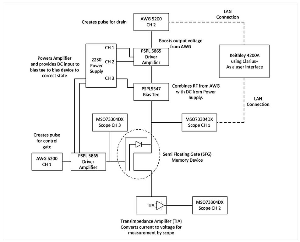
The solution illustrated in Figure 6 is being used by Fudan University (Shanghai) on their probe station. A recent publication, “A Semi-Floating Gate Transistor for Low-Voltage Ultrafast Memory and Sensing Operation,” outlines the testing on semi-floating transistors and the use of a transimpedance amplifier (TIA).
The measurement setup shown in Figure 7 includes an RF probe station, a pulse generator, a TIA, and a high-speed oscilloscope. The TIA shown was designed specifically for converting the current signal to voltage signal to view it on the scope.
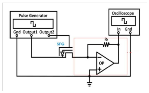
A TIA is a current-to-voltage converter. It's most often used in applications with sensors to amplify the current output of the sensor to a usable voltage.
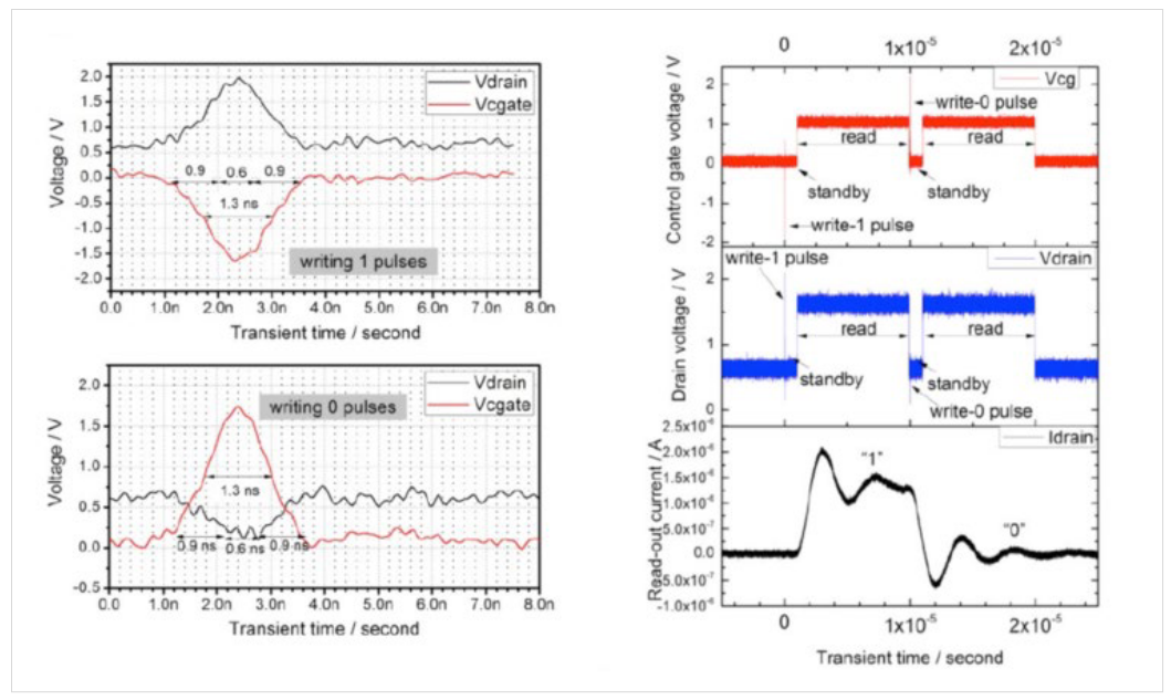
Figure 8 shows an example of the measured voltage signals seen at the scope. The drain voltage and the gate voltage are measured directly at the scope. The drain current is converted into voltage. Notice the pulse width is ~1 ns writing-1 pulse.
Two-Terminal Memory Cells
Other memory types, like the PCRAM, RRAM, MRAM, and STT-RAM, are based on a two-terminal memory cell. Figure 9 shows an example of testing done on PCRAM and that could also be applied to other two-terminal memory cells.
Chalcogenides-based phase change random access memory (PCRAM) holds great promise for high speed and large data storage applications. Chalcogenides are particularly noted for their varied responses to optical, electrical, and thermal stimuli.
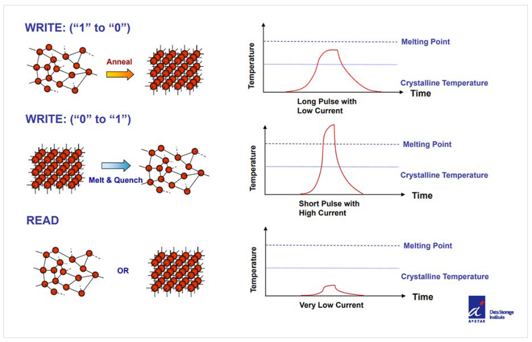
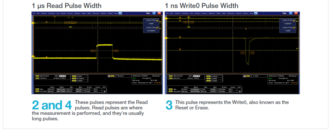
Figure 9 is a slide from a published work on "Phase Change Materials and PCRAM" by the Data Storage Institute. It shows the different pulse widths for read and write: a short pulse for "write" and long pulses for "read."
Figure 10 shows the PCRAM test setup with the Tektronix solution using a TIA. These memory cells are typically two-terminal devices. A constant voltage pulse is passed from the waveform generator through the whole circuit. The voltage pulse was measured before passing it through the memory cell. The current through the cell is then converted to voltage via the TIA and measured by the scope while the voltage pulse was applied. The voltage drop across the memory cell was then calculated by taking the difference between the voltages measured. The transient current was calculated, thereby allowing the transient resistance of the memory cell to be calculated.
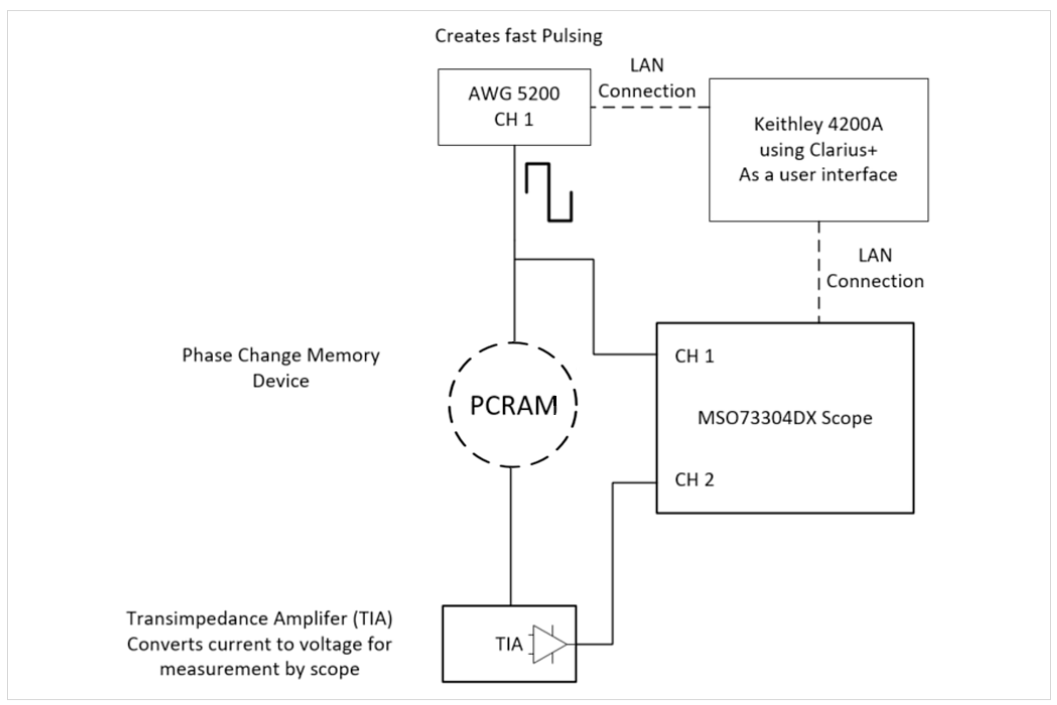
Depending on the voltage, there might not be a need for the PSPL amplifier shown in Figure 6.
Using the TIA offers two advantages:
- It would amplify the current output of the device to a usable and readable voltage on the scope.
- It could have a variable gain, which might be suitable for characterizing the PCRAM.
In-house Testing
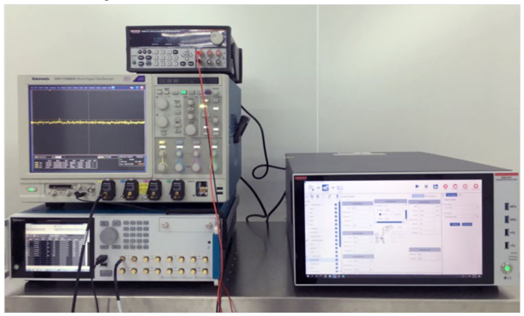
Figure 11 shows the test setup with MSO/DPO70000, AWG5200, and 2230 DC Power Supply. The Clarius+ Software in the 4200A-SCS Parameter Analyzer is used to control the instruments as a user-friendly GUI.
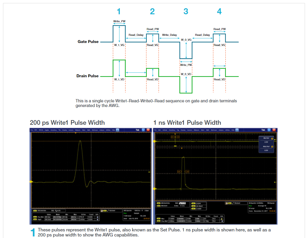
Figure 12 illustrates achieving the short pulse that is required for "write" and the long pulse required for "read."
This is the typical sequence for "write," "read," "erase," "read."
Additional testing was performed with a FEMTO® TIA with a bandwidth up to 4 MHz, as shown in Figure 13. Keithley modified and calibrated the TIA.
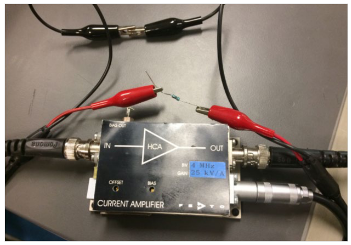
A 1 kΩ resistor was used in series with the function generator. The output was then connected to an oscilloscope, just as shown in Figure 10.
An input frequency of 1 MHz yielded the most stable waveforms, as shown in Figure 14.
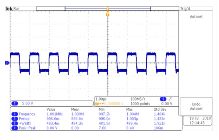
Notice the stable square wave amplified to 8 Vp-p. The pulse width is ~1 µs, which is desirable for the “read” part of the memory testing, given that this will be the measured part.
Additional testing was done on an evals TIA board. Figure 15 shows the TIA being powered by a Keithley 2220-30-1 dual channel power supply to convert the current output to a voltage output and amplify it to a degree which will be easily visible on the scope. A 50 Ω resistor that is connected to the TIA in series is acting as our device under test.
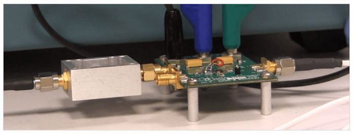
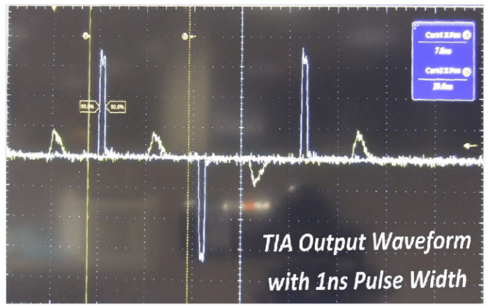
Figure 16 shows the TIA output waveforms at 1 ns. The blue waveform is the input of the AWG. The yellow waveform is the output of the TIA.
Conclusion
Ultra-fast (<10 ns) pulsing is required for the development of the newest nonvolatile memory types like Flash, PCRAM, STT-RAM and others. In addition to the recommended minimum and allowable minimum pulse widths possible using the Keithley 4225-PMU and 4225-RPM, this document offers an overview of an alternative method for ultra-fast measurement that could achieve pulse widths as short as <1 ns. This Tektronix solution includes a waveform generator, oscilloscope and off-the-shelf variable transimpedance amplifier, as well as a software package for easy interactive operation of all instruments.
Find more valuable resources at TEK.COM
Copyright © Tektronix. All rights reserved. Tektronix products are covered by U.S. and foreign patents, issued and pending. Information in this publication supersedes that in all previously published material. Specification and price change privileges reserved. TEKTRONIX and TEK are registered trademarks of Tektronix, Inc. All other trade names referenced are the service marks, trademarks or registered trademarks of their respective companies.
013119 1KW-61454-1

