Introduction
An increasing number of manufacturers are adding or retrofitting wireless technology into new or existing products. The products that are benefiting include mobiles, household, industrial, scientific, and medical devices. This technology transition is growing exponentially, however and with this growth come problems associated with Electromagnetic Interference (EMI). That problem, specifically, is EMI generated on the device’s board itself interfering with sensitive on-board cellular, GPS/GNSS, and Wi-Fi/Bluetooth receivers. This is called “platform” or self-interference and it’s become a big problem for manufacturers.
THIS APPLICATION NOTE
- Briefly describes wireless self-interference and its significance in IoT devices
- Defines broadband and narrow band interference and notes potential sources of each
- Provides techniques for observing potential sources using H-field probes and oscilloscopes with synchronized waveform and spectrum analysis capability
- Describes techniques using current probes and closespace antennas to look for EMI from cables and direct emissions in key communications bands
- Includes measurement examples using an LTEconnected IoT device
A 6 Series MSO was used to perform the measurements in this application note. Its low noise floor makes it especially suitable for measuring low signal levels. The ability to measure synchronized time domain waveforms and frequency domain spectrums is used in many of the techniques in this application note. This Spectrum View capability is also available in 4 and 5 Series MSOs, and the user interfaces are identical among these instruments. Hence, the same techniques may be used on the 4, 5, and 6 Series MSOs.
Wireless Self-Interference
The harmonic energy from digital clocks, high-speed data buses, and especially on-board DC-DC switch-mode power supplies can easily create interference well into the 600 to 850 MHz (and higher) cellular phones bands, causing receiver “desense” (reduced receiver sensitivity). This becomes especially challenging as the size of the product is reduced and noise sources become closer in proximity to onboard antennas.
In order to use the various mobiles phones services (Verizon, ATT, Sprint, T-mobiles, and others in the U.S. and other countries), manufacturers must pass very stringent receiver sensitivity and transmitter power compliance tests according to CTIA (Cellular Telephones Industries Association) standards. When on-board digital EMI and resulting receiver desense is discovered on a device, it can disrupt compliance testing to CTIA standards and often delay product introductions for weeks or months.
Cellular and wireless providers require a certain receiver sensitivity in dBm called Total Isotropic Sensitivity, or TIS. For example, this might typically be a sensitivity of at least -108 dBm, and must include the effect of antenna efficiency used in the mobiles device. Because mobiles device antennas typically operate in close proximity to human hands or head, this tends to reduce the sensitivity further (-99 dBm might be typical, depending on the antenna). More information on this, as well as the test methods, are described in CTIA’s “Test Plan for mobiles Station Over the Air Performance: Method of Measurement for Radiated RF Power and Receiver Performance” (Reference 1). Cellular radio manufacturer, Broadcom, also has some information in their white paper, Compliance with TIS and TRP Requirements (Reference 2).
Characterizing Self-Generated EMI
There are generally two primary areas of focus where onboard energy sources can couple to the receiver antenna or wireless module and cause loss of receiver sensitivity
(Figure 1):
- On-board energy sources, such as DC-DC converters, address and data buses, video cameras, and other fast-edged digital signals that can conduct or couple (capacitively or inductively) this EMI directly to wireless modules or their antennas. This is the most frequently encountered problem.
- Attached I/O or power cables that act as “radiating structures” (antennas) that couple this self-generated RF energy directly into on-board or attached wireless antennas.
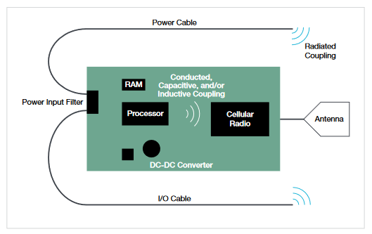
Using measurement techniques defined below, it is often possible to determine the sources of electromagnetic energy that could be coupling to on-board wireless receivers. Once the energy sources are identified and characterized, then the challenge is to determine how that energy is being coupled into the receiver and applying mitigating techniques for reducing the couplings.
Very often, the electromagnetic fields are coupled directly within the board, due to issues with stack-up, functional circuit partitioning (RF, digital, power conversion), or signal/power routing. It’s also very possible that stray electromagnetic fields are simply coupling directly into the antenna or transmission line. There could also be a combination of several coupling paths.
Types of Interference
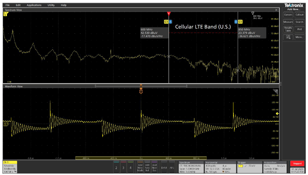
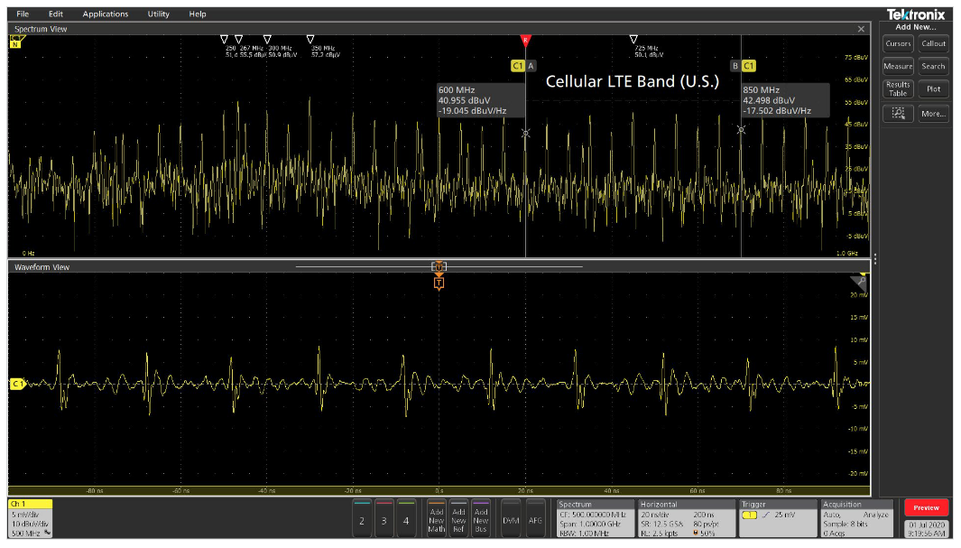
The two common types of high frequency harmonic signals that can disrupt sensitive receivers are narrow band and broadband. Figure 2 shows an example of broadband EMI from an on-board switching regulator as we’re looking from 1 to 1000 MHz. Figure 3 shows a typical narrow band clock over the same frequency range. Typically, DC-DC converters or data/address bus data will appear as a very broad signal with several resonant peaks, while crystal oscillators or highspeed clocks will appear as a series of narrow spikes.
Unless the product is designed for EMI compliance, both these types of signals can couple high frequency energy well into the mobiles phones or other wireless bands. Note the boundary for the U.S. LTE cellular band. Note that the broadband emission within the cellular band is on the order of 10 to 15 dB above the noise floor of the measurement system. The narrow band clock emissions are over 30 dB above the noise floor. Both these emissions will greatly affect reception at cellular frequencies if its allowed to couple to the receiver
Types of Measurements
There are three important steps in characterizing EMI at the board level for an IoT product; (1) use of near field probes to help characterize the sources of harmonic energy on the board or system, (2) a current probe to characterize the harmonic cable currents, and (3) a nearby antenna to monitor the actual emissions while troubleshooting. Optionally, you may use a TEM cell in place of the antenna
Step 1. Near Field Probes - There are three useful measurements for characterizing board-level EMI; (1) a general examination over a wide frequency range and (2) a narrower examination at just the receiver downlink band, and (3) an oscilloscope measurement of the DC-DC converter switched waveform.
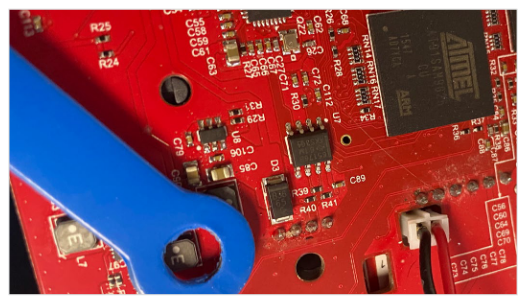
Since we’re wanting to couple to currents in traces and components, an H-field loop with about a 1 cm diameter is about the right size to identify and characterize EMI at the board level (Figure 4).
Start with A Wide Frequency Span - A wider measurement span (as in Figures 2 and 3) helps characterize the general profile of EMI sources, such as DC-DC converters, clocks, processor and memory bus noise, and any other potential high frequency device, such as Ethernet clocks. This measurement is taken from least 1 to 1000 MHz and will cover the U.S. cellular LTE bands. Try to identify the dominant harmonic energy sources that could be potentially coupling to the receiver module(s). Looking higher will include other wireless bands, but these on-board emissions seldom extend above 2 GHz. Placing Spectrum View in “Max Hold” mode is useful to indicate a maximum spectral amplitude.
Procedure - Connect a medium-sized (1 cm diameter) H-field probe to CH1. Double tap the CH1 badge to open the menu and set the Termination to 50 Ohms. Select the Spectrum View tab and turn ON Spectrum View in the upper-left. Leave the vertical scale set to “dBm” (default) and check off Normal and Max Hold. Next, double tap the Spectrum View menu and set the Span for 1000 MHz and the Center Frequency to 500 MHz. Set the Resolution Bandwidth (RBW Mode) to Manual and the RBW to 100 kHz. Probe each energy source (DC-DC converter, processor, memory, Ethernet clock, etc.) and set an appropriate Vertical and Horizontal Scale for a visible timedomain trace. Adjust the Trigger Level for a stable trace. Feel free to adjust the Span and Center Frequency higher to accommodate the GPS/GNSS band near 1575 MHz (or other wireless bands).
For example, measuring the processor/memory clock and DC-DC converter in a typical IoT device (Figures 2 and 3 above) using the H-field probe reveals a very high level of broadband and narrow band EMI from 1 to 1000 MHz. The U.S. cellular bands from 600 to 850 MHz are indicated by the two markers. The measured EMI is 10 to 30 dB over the ambient noise floor. If this EMI were to couple to the receiver input, it could cause severe receiver desense.
Narrow the Span to the Downlink Band - Once the dominant harmonic energy sources on the board are identified and characterized, the second useful measurement is to narrow the span and look at just the receiver (downlink) band using the same near field probe in various locationss. A chart of cellular LTE bands in the U.S. may be found in Reference 3. For example, a common downlink band for Verizon LTE in the U.S. would be “Band 13” of the FCC allocations from 746 to 756 MHz (Figure 5). By probing all the remaining circuitry, you may be able to identify other potential interfering sources.
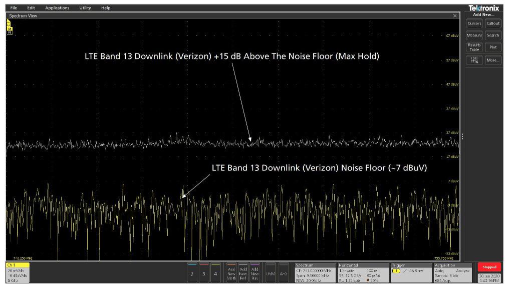
You may need to make these measurements inside a shielded room in order to exclude other mobiles phones transmissions from disrupting your measurements.
Characterize DC-DC Converter Ringing and Rise Times – The third useful measurement using the H-field probe is to characterize the switching waveforms of the various DC-DC converters in the time domain. This is important for identifying ringing on the switched waveform, because this ring frequency can translate to broad peaking in the emission and EMI coupling characteristics. Sometimes these broad peaks in emission coincide with cellular bands. H-field probes are quick and safe because they don’t require direct connection to the circuitry – just couple it to the output inductor.
Using an H-field Probe to Examine DC-DC Switching Characteristics
In order to show that using an H-field probe provides valid characterization measurements let’s examine the math. Refer to Figure 6. There will be some unknown mutual coupling factor (M in the equation) between the inductor and H-field probe. Because we don’t know the mutual coupling factor, the amplitude won’t compare with actually measuring with an oscilloscope probe. However, for EMI purposes we’re mainly interested in the rise time, general switched wave shape, and ringing frequency, if any
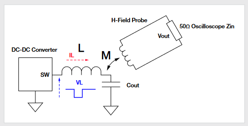
A DC-DC converter usually has a near square wave signal (vL) from the converter switch node (SW) and output inductor (L) input to ground return and this is what we’d measure with an oscilloscope probe. The current through the inductor is related to that voltage as:

Assuming the H-field probe is held close to the inductor, we get some mutual coupling, M (unknown) and the output of the probe is:

Combining equations 1 and 2, we get:

Using the non-invasive H-field probe measurement, most important characteristics for EMI are now easily and quickly measured without the risk of shorting connections with oscilloscope probe tips during circuit operation. By using the H-field probe held close to each DC-DC converter inductor, we can measure the rise time, pulse width and period, and ringing frequency.
| Measurements | Importance |
| Rise time | Indicates the upper range of harmonic frequencies |
| Pulse width and period | Factors into harmonic frequencies |
| Ringing frequency | Can cause broad resonant peaking in the broad band spectrum |
Table 1: H-field probe measurements and why they are relevant.
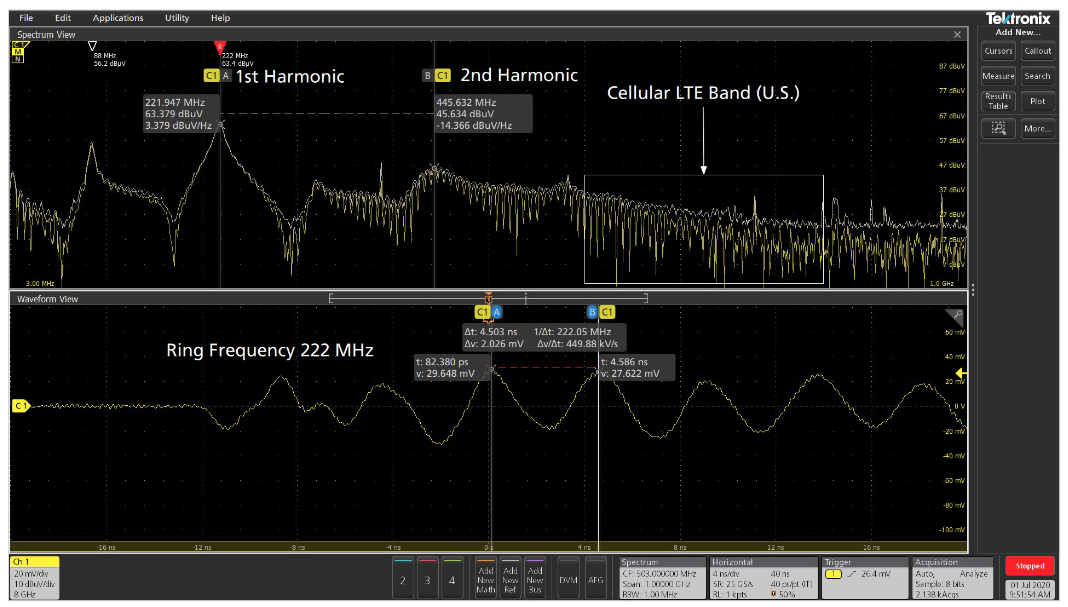
In Figure 7, we see a rather extreme example of ringing from a DC-DC converter. The ring frequency is 222 MHz and the resulting EMI peaks at this ring frequency. The second harmonic at 444 MHz is also readily visible. If these ring-related peaks were to occur within one of the wireless bands used, receiver sensitivity would certainly suffer.
Step 2. Current Probes - Figure 9 shows how a current probe is used to measure the common mode harmonic currents flowing along a power cable to a cellular LTE wildlife camera. How these currents are formed and why they tend to couple onto cables is explained more completely in References 4 and 5. Let’s just assume that small RF common mode currents generated on the PC board (usually in the microamp range) can easily couple to attached I/O and power cables, which can then re-radiate into the radio module as we saw modelled in Figure 1 previously.
The 4, 5 and 6 Series MSOs with Spectrum View are useful tools for these measurements (Figure 8). The current probe can measure RF common mode currents in either power cords or I/O cables. Either can radiate directly to IoT antennas.
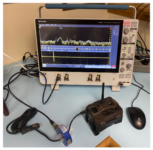
Use of the current probe will help determine whether a given power or I/O cable might be contributing to the overall EMI coupling issue. Use the same basic procedure described above to display harmonic currents in cables using a current probe.
Most portable wireless or cellular products will have, at most, a DC charging cable, but probably no I/O cables. A good troubleshooting technique would be to simply remove all cables and repeat the receiver sensitivity testing to see if the interference clears up. It is much more likely any selfgenerated EMI couplings will be within the PC board itself.
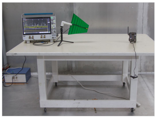
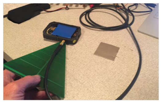
Step 3. Close-Spaced Antenna - to measure the direct emissions from a wireless device with or without cables attached, you may use a close-spaced antenna (typically, 1 m distance) to pick up the emissions (Figure 9). The antenna does not need to be calibrated or even resonant over the entire frequency range, just positioned at a close enough distance where harmonic emissions may be observed. The antenna may need to be positioned closer than 1m to observe the emissions from self-interference (Figure 10).
The most important harmonic frequencies to monitor would include the cellular LTE bands (approx. 600 to 850 MHz), the commercial GPS L2 frequency of 1575.42 MHz, the higher cellular bands around 1.8 to 1.9 GHz, and the Wi-Fi ISM band of 2.4 to 2.5 GHz. On-board harmonic content seldom goes higher than that.
In the case of the mobiles device in Figure 10, there was leakage observed from the internal video camera radiating out the edge of the PC board assembly. The cellular antenna was embedded within the case and located close to the board edge.
Summary
Wireless self-interference has quickly become one of the most challenging issues for manufacturers developing wireless and IoT products, especially for those desiring to utilize the cellular system. Success depends on carefully designing the entire product to ensure minimal self-generated EMI. Proper circuit board layout and stack-up are key factors for success. An oscilloscope that can display both time and frequency domain, such as the Tektronix 4/5/6 Series MSOs with Spectrum View is very useful in characterizing and debugging self-generated EMI.


